SK Hynix (SKHY) is spending more than $4 billion to build its first U.S. high-bandwidth memory production hub, a major bet on the artificial intelligence boom.
But a big chunk of those chips will still have a voyage of thousands of miles before them.
South Korea’s semiconductor behemoth broke ground in August on an advanced packaging plant in West Lafayette, Ind., that is slated to start mass production of next-generation high-bandwidth memory in the second half of 2029.
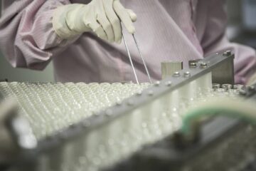
The facility will package and test the advanced memory used alongside processors that power artificial intelligence systems.
Well, there’s a catch.
The Indiana factory will initially receive state-of-the-art wafers made at SK Hynix’s plants in South Korea. The wafers will be sent to Indiana for advanced packaging and testing, after which final goods will be shipped to U.S. consumers.
That makes SK Hynix’s recently reported discussions with Intel (INTC) more fascinating.
Three sources told Reuters that SK Hynix is in talks with Intel over a deal that could see it manufacture memory chips in the U.S. for the first time.
What exactly SK Hynix might produce there is not known.
But if the conversations ultimately lead to more sophisticated memory wafer production in Ohio, Intel could possibly offer something SK Hynix’s $4 billion Indiana project doesn’t: front-end memory manufacture on U.S. territory.
SK Hynix’s Indiana AI plant still starts with Korean wafers
SK Hynix’s investment in Indiana is huge.
The company announced that it plans to spend over $4 billion on the West Lafayette facility. Mass production of next-generation HBM is expected in the second half of 2029 after its cleanroom opens in October 2028.
During commercial operations, the project is estimated to produce around 1,000 jobs, while SK Hynix predicts some 7,000 direct and indirect jobs would be created via construction and operations.
The facility will also house a state-of-the-art packaging research and development testbed developed in collaboration with Purdue University.
HBM is a vital component of the AI infrastructure explosion.
Rather than depending on traditional memory that is located farther away from the CPU, HBM stacks memory dies on top of each other, giving the massive bandwidth AI accelerators need.
As expenditure on AI infrastructure surges, SK Hynix has become one of the major producers of HBM in the industry.
Related: SK Hynix’s $38 billion buildout has a name attached: Nvidia
The Indiana plant handles one key aspect of that manufacturing process, but not the whole thing.
Advanced packaging is a backend semiconductor technique that integrates, or vertically stacks, many chips into one package, SK Hynix said. The advanced wafers Indiana will package and test are likely to arrive from South Korea.
SK Hynix spelled out the production chain openly with the Indiana landmark announcement.
The latest wafers created in Korea will be sent to Indiana, where the business claims they will be given sophisticated packaging and testing before the final “Made in USA” items are provided to American consumers, SK Hynix said.
That offers SK Hynix an American HBM production operation but doesn’t erase the company’s need for South Korean front-end manufacturing.
And that’s where Intel’s Ohio initiative might be important.
Intel’s Ohio factories could fill a different part of the chain
Intel always envisioned its Ohio project as much more than a packing plant.
The business is constructing two state-of-the-art semiconductor plants on over 1,000 acres in New Albany, Ohio.
Intel expects to spend more than $28 billion on the first two plants, and the site has potential for up to eight chip plants and related facilities in the future. Intel has previously said that the overall investment may reach as much as $100 billion when fully built out.
It’s been timing.
Intel revealed its Ohio intentions in 2022, but the corporation has continually delayed the production timetable for the project.
The present aim is to finish construction of the first production module, the so-called Mod 1, by 2030. The start of operations is scheduled between 2030 and 2031.
Mod 2 is planned to be complete in 2031 and to begin operations in 2032.
That pricey, time-consuming manufacturing footprint is now front and center in the SK Hynix conversations.
More AI:
- Nvidia just made a move Wall Street wasn’t ready for
- Microsoft just took sides in AI policy fight
- OpenAI just disclosed something genuinely alarming
One possibility may be SK Hynix leasing some of Intel’s Ohio plant, Reuters said.
Another scenario would be a consortium of SK Hynix, Intel, and large cloud computing businesses wanting to lock in memory-chip supply as demand for AI infrastructure rises. The discussions remain exploratory, and no decision has yet been made.
There’s a clear strategic decision.
If SK Hynix ends up developing its U.S. HBM plant in Ohio to produce the advanced memory wafers it needs, the firm may possibly shift another key element of its AI-memory supply chain from South Korea to the U.S.
Ohio could handle front-end wafer fabrication. Indiana could handle advanced HBM packaging and testing. Finished memory could then move to U.S. customers driving the AI infrastructure buildout. But that scenario is not yet an announced plan.
Reuters was unable to establish what kind of memory SK Hynix might manufacture in Ohio. Its product portfolio includes conventional DRAM, NAND flash, and HBM, and the company has not said which, if any, would be involved in an Intel agreement.
That caveat is crucial: Ohio supplying Indiana is a potential strategic fit based on the functions of the two facilities, not something Intel or SK Hynix has announced.

Intel and SK Hynix have a timing problem
There’s another reason a supply chain from Ohio to Indiana is still speculative.
SK Hynix’s most sophisticated technology is of critical importance to South Korea.
Any deal incorporating sophisticated memory like as HBM or DRAM might face objections from Seoul, the three sources familiar with Intel’s negotiations said.
The South Korean trade ministry said it would be up to a business to decide to build chips in the U.S. but that a transaction involving a designated “national core technology” would be subject to examination under the country’s Industrial Technology Protection Act.
It’s not only an issue of whether it makes financial sense for SK Hynix to build another facility.
It is caught between rival industrial interests.
The U.S. aims to boost semiconductor production at home, with AI driving demand for chips and memory.
South Korea aims to safeguard key semiconductor technology and ensure investment in its manufacturing environment. Meanwhile, SK Hynix clients desire greater supply.
The corporation has recognized pressure.
In July, SK Group Chairman Chey Tae-won said SK Hynix was under huge pressure and lobbying from its customers and governments to make more chips. He also said he felt the corporation needs to create a U.S. facility if feasible, Reuters reported.
The economics complicate the choice.
The cost of making semiconductors is much greater in the U.S. than in South Korea due to higher labor and building expenditures. Asia also concentrates much of the semiconductor industry’s supply chain.
But manufacturing costs are only one part of the calculation. AI customers want more memory capacity. SK Hynix wants to remain a leading supplier to those customers.
Intel has billions of dollars invested in a manufacturing site that has missed its intended timeline again and again.
Those interests provide the corporations a motivation to continue negotiating even if the end result looks considerably different from the options on the table now.
Intel could give SK Hynix something Indiana cannot
The importance of a possible Intel merger becomes evident in the light of the two U.S. initiatives.
SK Hynix has already pledged more than $4 billion to Indiana. That facility will do a crucial technical element of HBM production: sophisticated packaging and testing.
But SK Hynix’s own production strategy keeps the start of the process in South Korea. There, state-of-the-art wafers will be made and sent over the Pacific to be processed into next-generation HBM in Indiana.
Intel’s Ohio plants are built for a very different purpose: front-end semiconductor production.
This results in a potentially complementary production footprint.
If the firms finally determine Ohio should make advanced memory wafers vital to SK Hynix’s HBM activities, part of the supply chain presently running from South Korea to Indiana may be squeezed inside the American Midwest.
But investors shouldn’t count on it for three reasons:
First, the discussions are exploratory.
Second, SK Hynix has maintained that nothing is decided in terms of collaboration with the businesses named in the Reuters story or U.S. memory-chip manufacture.
Third, Reuters was unable to identify what sort of memory will be produced at Intel’s Ohio plant if a deal is completed.
The timescales also point to any deal being more about the future of the business than an urgent response to today’s supply concerns.
Mass manufacturing is planned for Indiana in the second part of 2029. Intel expects to bring the first Ohio production module online in 2030 or 2031.
If these plans are realized, Korean wafers will remain essential to SK Hynix’s first U.S. HBM manufacture.
But the negotiations with Intel are an indication of how that setup may one day develop.
SK Hynix has a location in mind for packaging and testing sophisticated AI memory on American soil.
What it has not done is bring back to the U.S. the manufacture of the cutting-edge wafers that feed that operation. Intel’s massive Ohio project might provide a means to achieve just that.
Related: Intel stock jumps as SK Hynix weighs U.S. memory-chip deal